In this article, let us look at the Quad-SPI interface, and learn how it works!
If you have just mastered this SPI interface, then looking at Dual and Quad SPI can be overwhelming. I had to read several pdfs to wrap my mind around this concept. In this article, I am presenting all the useful and interesting facts on Quad-SPI that I have learned through my research.
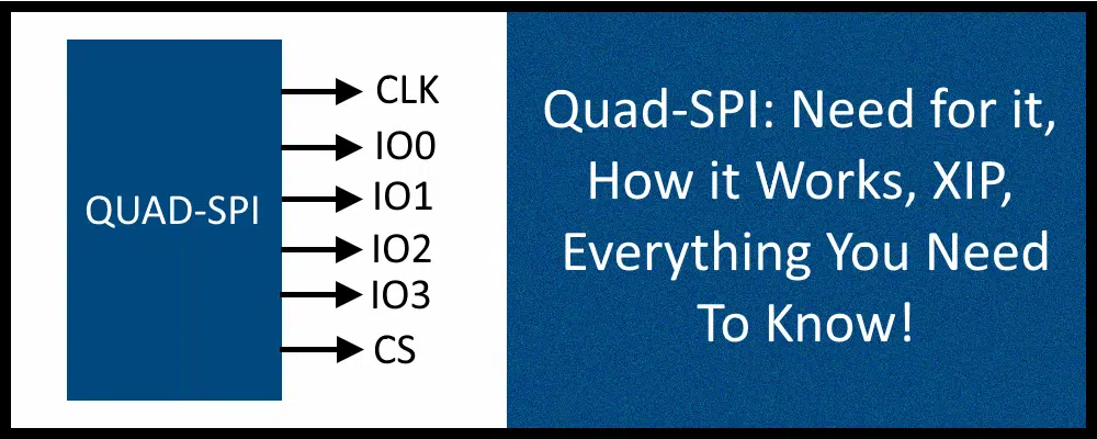
What is Quad-SPI? It is a serial interface, where 4 data lines are used to read, write and erase flash chips.
Quad-SPI
Quad-SPI, also known as QSPI, is a peripheral that can be found in most modern microcontrollers. It has been specifically designed for talking to flash chips that support this interface. It is especially useful in applications that involve a lot of memory-intensive data like multimedia and on-chip memory is not enough. It can be also used to store code externally and it has the ability to make the external memory behave as fast as the internal memory through some special mechanisms.
It is faster than traditional SPI as quad-SPI uses 4 data lines (I0, I1, I2, and I3) as opposed to just 2 data lines (MOSI and MISO) on the traditional SPI.
Let’s see further in detail about the following in this article.
- need for quad-SPI,
- how quad-SPI works,
- what is double data rate mode,
- what is XIP, and
- advantages of Quad-SPI over SPI and parallel memory.
Need for Quad SPI
Why did the damn engineers come up with yet another protocol? Wasn’t SPI with speed up to 16Mbps enough for all applications?
SPI was enough for most of the use cases like reading data from sensors and sending data to actuators or output devices and is still one of the most preferred protocols for on-chip serial communication. But engineers struggled with one important problem, which is adding more memory to their embedded devices.
What is the problem with flash memory, that makes it need a special interface? Flash memory is cheap and durable which makes it an attractive option for embedded applications. But it is slow by nature and this will create a bottleneck and impact the performance of embedded applications. Even though SPI is fast and can go up to 16MHz, the flash devices were not able to send out data at this rate through a single data line to make it work as fast as the on-chip memory.
What solution did we use before quad SPI? Earlier before quad-SPI came, the solution was to use parallel memory where 8, 16 or 32 pins (depending on the address range) can be used to connect the external memory device with the microcontroller to achieve fast performance. But this approach had 2 major cons
- It made the PCB design complicated.
- It also meant that all these pins are fixed to one particular chip and cannot be used anymore for literally anything else.
Due to all of these problems, engineers needed to come up with a proper solution for making flash faster and the solution they came up with is to just modify the SPI protocols to use 2 more data lines and make all 4 data lines bidirectional and they named it Quad-SPI.
How Quad-SPI works?
Unlike normal SPI which uses separate data lines for input and output (MISO and MOSI), the Quad-SPI interface configures the data lines on the fly so that they act as outputs if we need to send some information to the flash memory and they can act as inputs if we need to read some memory contents.
It uses 4 data lines namely I0, I1, I2 and I3 as shown in the figure (courtesy STMicroelectronics).
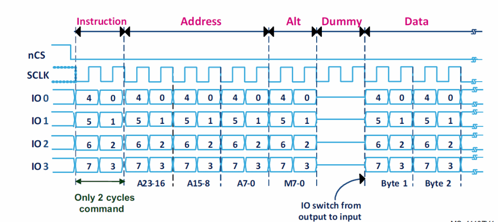
The figure shows the typical stages of a Quad-SPI exchange. First, the instruction is sent over the IO lines. Followed by the address and then comes the Alt field which can be implemented the way the manufacturer of the flash memory wants it to be. Then for a brief period, 2 clock cycles in the above figure, the transmission is paused to allow for changing the direction of the I/O line. Then the data is sent from the flash device to the microcontroller.
As you can see 4 bits are transferred every clock cycle. The bit order as you can see is IO0 sends bit0, IO1 sends bit1 and so on in the first clock cycle and bits 4,5,6, and 7 are sent out in the 2nd clock cycle. Thus in just 2 clock cycles, the entire byte is transmitted!
What is Double Data Rate Mode?
Traditionally the value on the data line is changed at either the rising edge or the falling edge of the clock. This is also known as the Single Data Rate mode. You can see that in the figure below.
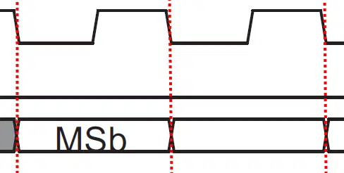
As you can see in the above pic (courtesy Cypress), here the sender changes the voltage on the data line at the falling edge of every clock period. In other words, it sends one bit per clock cycle.
In double data rate mode, the voltage on the data line is changed in both the rising edge and the falling edge, which allows the device to send 2 bits per clock cycle and thus doubling the speed of transmission.
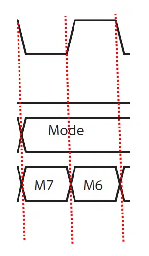
As you can see in the pic (courtesy Cypress) above the data is sent 2 bits per clock cycle (the signal on the top is the clock signal), this is how the double data rate mode works. This mode needs to be supported on both sides of the communication channel i.e. both the microcontroller and the flash chip need to have inbuilt support to implement this mode of operation.
What is XIP?
XIP stands for eXecute In Place, it is a feature which allows the microcontroller to execute code straight from the external flash memory without copying it first. This allows for faster and more efficient execution of code.
When the code size gets too big to be stored in the on-chip storage, we usually go for external memory, but the problem with external memory used to be the fact that it was very slow to access. But using Quad-SPI mode and a prefetch mechanism, the data retrieval speed of external flash devices can be made comparable to the on-chip storage and hence can be used to not just store some databases and multimedia but it can be used to execute code too.
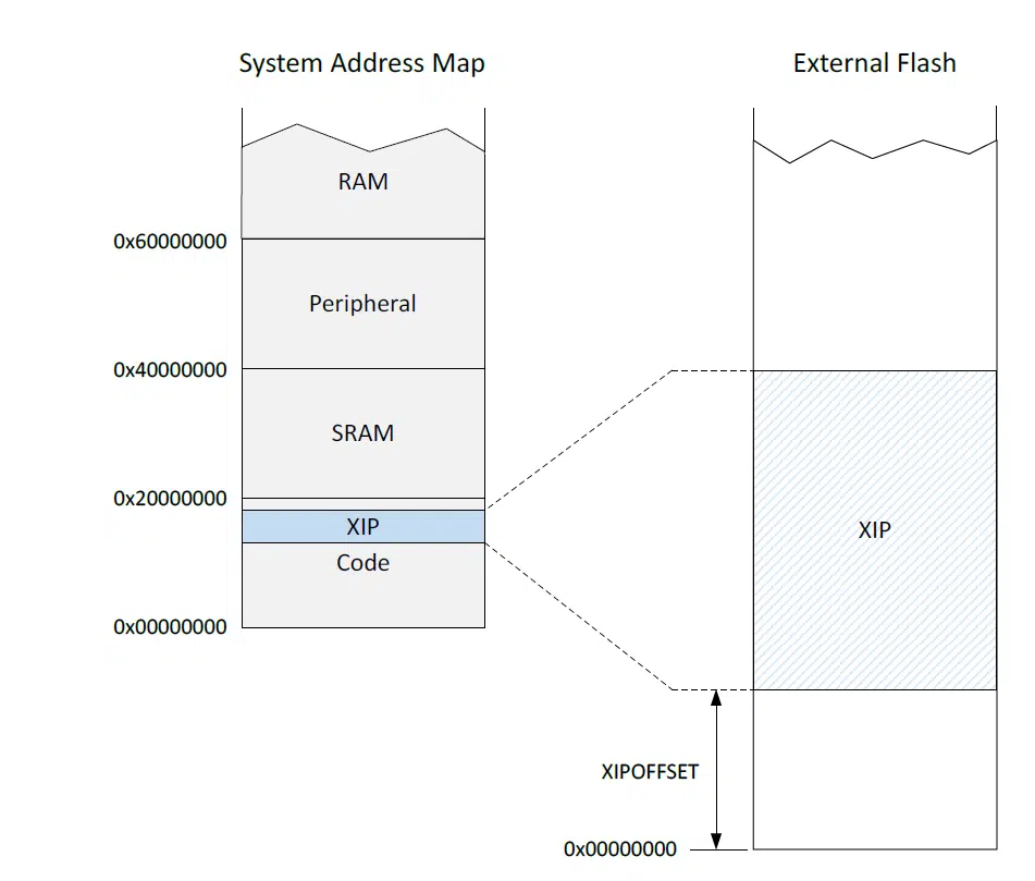
As you can see in the above picture (Courtesy Nordic Semiconductors ), this is usually done by memory mapping the flash storage addresses onto the processor’s memory space. This creates an illusion so that from the perspective of the processor, the memory on the external flash device is just another location on its on-chip memory!
Advantages of using Quad-SPI
Some of the advantages of Quad-SPI mode include the following.
- lower pin count as compared to parallel memories, which means there are more GPIO for other uses
- easier to design the PCB which is a direct consequence of lower pin count, which further leads to the lower overall cost of development
- more compact design can be achieved as opposed to parallel memory options
- multiple devices can be linked to a single Quad-SPI interface and the same data lines can be connected to multiple devices. To select a particular chip, the chip select pin can be used. This is an advantage since if we use a parallel memory solution we need a separate set of data lines for each chip we interface with.
- approximately 4 times more throughput can be achieved as compared to SPI
- has support for executing code in place through XIP, which can help increase the code memory and efficiency of complex systems
Related Questions
What is dual SPI? Dual-SPI is another variation of SPI that came before quad-SPI which, as the name implies, uses 2 data-lines to transfer data (instead of 4 as in quad-SPI).
Usually, flash-chips that support quad-SPI also support dual-SPI. It is basically a tradeoff between the pin count and data transfer speed.
Are SPI and QSPI pin-compatible? Most flash chips these days have a pin layout that lets the user decide to either use it as normal SPI or Quad SPI.
This is because several older applications are still stuck on an SPI interface and the implementation of moving to quad-SPI is still in their Todo lists! Also, another reason is that some older and less complex microcontrollers still do not have a quad-SPI interface, so by giving both options the flash chip makers can support a wider variety of microcontrollers.
I hope you enjoyed reading this article and got some value out of it!
Feel free to share it with your friends and colleagues!
If you have any questions or sugessions you can also email us or contact us through this link!